1. General info
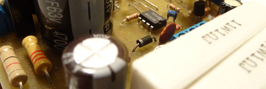
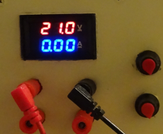
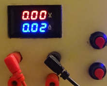
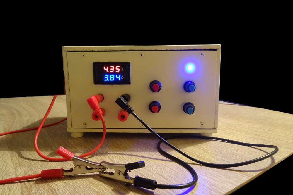
This is a laboratory power supply with a stabilized output, continuously adjustable from 0-20 VDC and 2 mA - 4 A. The built-in current limiter makes it particularly useful when experimenting with electronics, as you can set a maximum current before applying voltage - protecting both the circuit under test and the supply itself. Additional protections guard against component failure and output overload.
The power supply operates in two modes:
- Voltage source: The output voltage is fixed and set by the red potentiometers.
- Current source: The output current has reached the limit set by the blue potentiometers. The blue LED lights up, and the voltage is regulated automatically to keep the current at the set value.
This design is based on a modified circuit originally published at www.electronic-lab.com. The same circuit is widely available as a commercial DIY kit and is very popular among hobbyists. Circuit simulations were performed in EveryCircuit and schematic drawings were created with EasyEDA - both free, web-based tools.
2. Schematics
The full circuit can be broken down into four functional blocks:
- Rectifier and stabilized supply with a negative rail - powers the circuit internals and the output stage.
- Voltage reference - provides the stable reference that the output is regulated against.
- Output amplifier - amplifies the reference voltage to drive the output.
- Current limiter - monitors the output current and switches the supply into constant-current mode when the set limit is reached.
2.1. Rectifier with a negative rail
The supply is powered by a step-down mains transformer with two 18 VAC / 2 A secondaries. Connecting them in parallel gives 18 VAC at 4 A. Since 18 VAC is an RMS value, the peak voltage is √2 × 18 V ≈ 25 V - this is the voltage the filter capacitors charge to, which translates to roughly 20 V at the output under load.
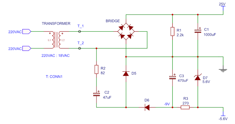
A standard Graetz bridge rectifier (rated for at least 5 A) together with capacitor C1 form a full-wave rectifier to produce a DC rail. The op-amps used in this design (type 741) can only swing their output down to a few volts above their negative supply, so a small negative rail is needed to allow the output to reach true zero. This is achieved by the negative rail sub-circuit.
In steady-state operation the negative rail works as follows: C1 is charged to approximately 25 V. Secondary terminal T2 swings ±25 V relative to the chosen ground. During the positive half-cycle, current flows from T2 through C2 and D5, charging C2. During the negative half-cycle, current flows from ground through D7 into C3 (charging it), then through D6, discharging C2. The voltage across C3 stabilises at about 9 V, set by the Zener diode current: 5.6 V + 12.5 mA × 270 Ω ≈ 9 V. C2 oscillates around 16.5 V as it charges and discharges each cycle. See the simulation of the sub-circuit.
2.2. Voltage reference
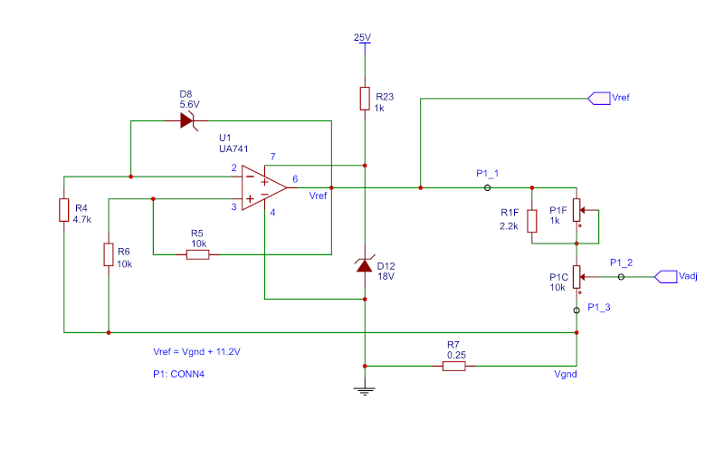
The voltage reference is built around D8, a 5.6 V Zener diode operated at its zero temperature coefficient current. At this specific operating point, two competing breakdown mechanisms - reverse-biased breakdown (negative temperature coefficient) and avalanche breakdown (positive temperature coefficient) - cancel each other out, making the reference voltage virtually independent of temperature.
Op-amp U1 amplifies the 5.6 V reference by a factor of 2, set by the resistor divider R5/R6 in its positive feedback path. Importantly, the reference is biased against the output ground of the power supply (Vgnd) rather than the circuit ground. The difference between the two ground potentials is developed across the ballast resistor R7, through which all output current flows. At the maximum rated output of 4 A, this offset stays below 1 V.
The amplified reference voltage Vref is then scaled by two potentiometers: P1C (coarse) and P1F (fine), both mounted on the front panel. The fine adjustment spans 0-687 Ω in parallel with a fixed resistor. Because of this parallel combination, the fine control is non-linear - it responds faster near zero and slows down as the resistance approaches 687 Ω. The resulting adjusted voltage Vadj is fed into the next stage, which amplifies it (approximately 3×, adjustable) and drives the output transistors.
2.3. Output amplifier
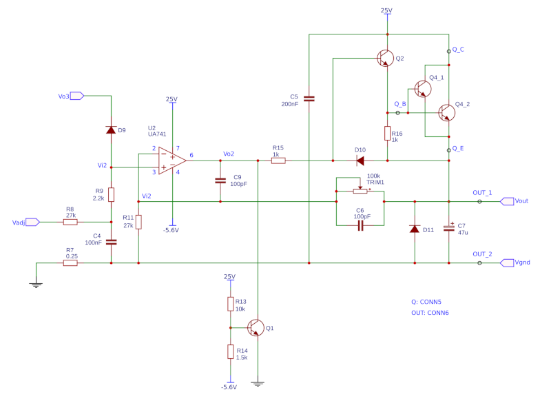
The output stage is built around op-amp U2, configured as a voltage amplifier with adjustable gain, followed by a pair of buffer transistors that boost the output current. The adjusted reference voltage Vadj from the previous stage is fed into the positive input of U2. When the current limiter is active, Vadj is overridden by the output of U3 (Vo3): if Vo3 is low enough to forward-bias D9, it takes control of the positive input. In both cases the voltage at U2's positive input is Vi2 - equal to Vadj in voltage-source mode, or Vo3 + 0.7 V in current-source mode.
U2 drives its output (pin 6) until its negative input matches Vi2, producing an amplified output voltage Vo2 = Vi2 × (TRIM1 + R11) / R11. Trimmer potentiometer TRIM1 allows the gain to be calibrated so that P1 sweeps its full range; with Vref spanning 0-11.2 V, TRIM1 is set close to R11 in value, giving a gain of approximately 2. This gain applies only to the DC component - fast transients bypass the feedback network through C6 and are attenuated. Input noise on Vadj is suppressed by C4, and any high-frequency disturbances generated by U2 itself are fed back through C9 and cancelled at the negative input.
The circuit around Q1 protects the supply from a failure of the negative rail. If the −5.6 V rail collapses, the base-emitter junction of Q1 becomes forward-biased, saturating it. This pulls the base of Q2 low, cutting it off and in turn switching off Q4, preventing any damage to the output stage.
Output current amplification is handled by the Darlington pair Q2 and Q4. Q2 is necessary because U2 alone cannot source enough base current to keep the power transistor Q4 (2N3055) in its active region at full load. C7 filters high-frequency noise on the output, and D11 is a flyback diode that clamps negative voltage spikes from inductive loads.
2.4. Current limiter
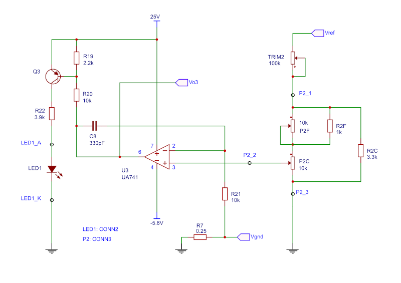
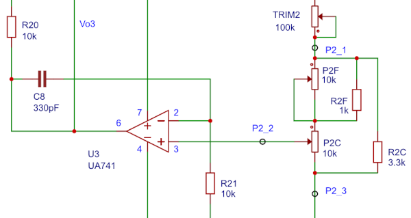
The current limiter is built around U3, which operates as a voltage comparator. Under no-load conditions, with zero output current, U3 holds its output (Vo3) high at approximately 25 V. At this level D9 is reverse-biased, so Vo3 has no effect on the output amplifier U2 (see section 2.3).
As the output current increases, the voltage drop across ballast resistor R7 raises Vgnd above the voltage on U3's positive input. Once this threshold is crossed, U3's inputs are in reverse polarity and its output swings from +25 V to a negative value. This forward-biases D9, connecting Vo3 + 0.7 V directly to U2's positive input and overriding the voltage reference — the supply has entered current-source mode. U2 then regulates the output voltage downward to whatever level keeps the current at the set limit.
3. Assembly
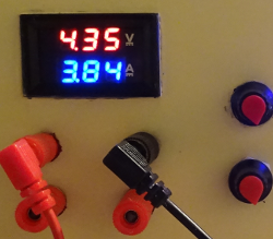
For display we use cheap voltage and current meter. The meter used here has two lines for powering the meter (red and black) and three lines used for measuring in a common cathode connection (red, blue and black). We can connect the measuring lines as shown in the above image. The meter needs a power supply (from 4.5V to 30V DC), we can use a 15V from a standard regulator 7815.
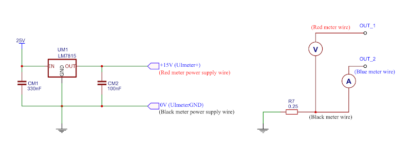
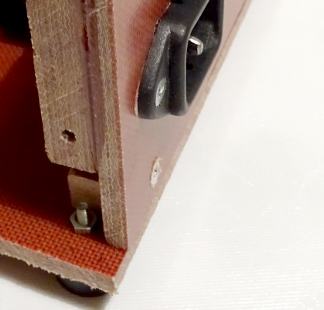
This is the assembly of the external parts of the circuit to the PCB. I made the case from textolite sheets that have beams on their sides through that connect with other sheets. Beams are drilled and glued with epoxy resin. This makes the bond strong enough to carry the construction.
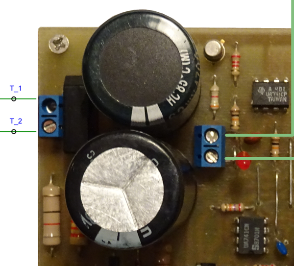
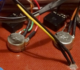
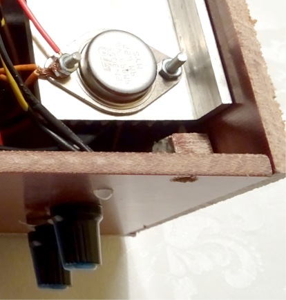
The enclosure is tightly packed but holes for air circulation around the transistors must exist.
4. Downloads
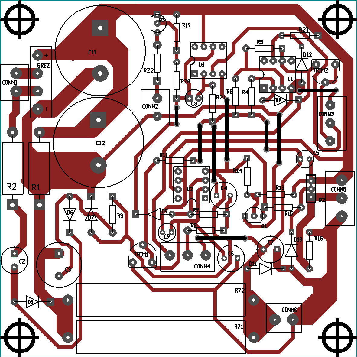
Here are files for the PCB and assembly. The PCB is designed in EasyEDA, which allows you to export it in various formats. The assembly file is a PNG image showing the placement of components on the PCB.